Google is assembling a custom chip supply chain involving four design partners, a fabrication relationship with TSMC, and a product roadmap extending from inference chips shipping today to 2-nanometre processors the company expects to deploy in late 2027. The strategy was detailed in a Bloomberg feature published ahead of Google Cloud Next and reported separately by The Next Web, the Los Angeles Times, and Business Today.
Ironwood Targets Inference Workloads
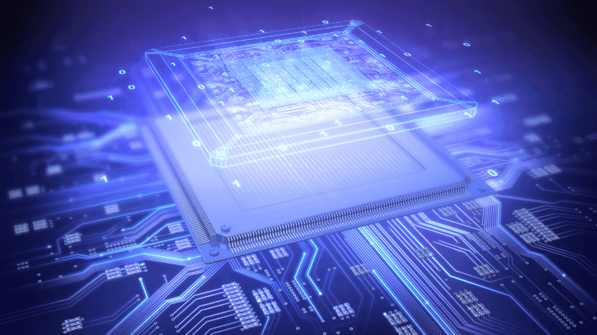
The centrepiece of the current generation is Ironwood, Google's seventh-generation TPU and the first the company describes as designed specifically for inference — the phase of AI computing where trained models serve user queries rather than learn from data.
According to Google's product disclosures cited by Bloomberg, Ironwood delivers ten times the peak performance of the TPU v5p, carries 192 gigabytes of HBM3E memory per chip with 7.2 terabytes per second of bandwidth, and scales to 9,216 liquid-cooled chips in a single superpod producing 42.5 FP8 exaflops. Ironwood is now generally available to Google Cloud customers.
Google says it plans to produce millions of Ironwood units this year. Anthropic has committed to up to one million TPUs, according to Bloomberg, and Meta has a rental arrangement for capacity.
Four Design Partners, Split Workloads
Google's chip programme now involves four distinct design partners handling different segments of the product line, according to Bloomberg and The Next Web.
Broadcom signed a long-term agreement to supply TPUs and networking components through 2031, according to The Next Web, which reports the deal was signed on 6 April. DeepBrief has not independently verified the agreement date against Broadcom regulatory filings. Broadcom is also designing the next-generation TPU v8 training chip, codenamed "Sunfish."
MediaTek is designing an inference-focused chip codenamed "Zebrafish," which The Next Web reports targets 20–30% lower cost than comparable training-oriented silicon. Marvell is in talks with Google to supply a memory processing unit and an additional inference TPU, as covered in DeepBrief's earlier reporting on the Google-Marvell custom inference chip negotiations. Intel rounds out the design roster, according to Bloomberg.
TSMC is the fabrication partner across the roadmap, with the TPU v8 generation targeted for its 2-nanometre process in late 2027, according to the Bloomberg feature.
Customer Commitments and Deployment
Bloomberg and the Los Angeles Times both report that Anthropic has committed to deploying up to one million TPUs, a figure Anthropic has disclosed publicly. Meta's arrangement is described by Bloomberg as a rental of TPU capacity rather than a direct purchase.
Google's approach contrasts with hyperscaler peers that have concentrated their custom silicon work with a single partner. Meta has detailed its own custom chip efforts as part of a broader infrastructure stack, which DeepBrief covered in its report on Meta's AI stack and custom silicon plans.
Inference Market Structure
The inference segment of the AI accelerator market has attracted new entrants and product launches over the past year. Nvidia announced an inference-oriented product at its GTC conference, which DeepBrief reported on in its coverage of the Nvidia Groq 3 LPU launch.
Nvidia did not provide a comment in response to questions about Google's supply chain plans, according to Bloomberg. DeepBrief was unable to obtain an independent chip analyst on the record in time for publication and is not characterising the competitive posture of the market beyond the structural facts disclosed by the companies involved.
Google's public positioning, as reported by Business Today and TweakTown, frames the custom chip effort as a vertically integrated alternative for cloud customers running inference workloads. Neither outlet quotes Nvidia or an independent analyst on the specific claims.
Timeline and Capacity
Per Bloomberg, Google's roadmap moves from Ironwood in general availability today to the Broadcom-designed "Sunfish" TPU v8 training chip and MediaTek-designed "Zebrafish" inference chip in the next generation, with the 2nm TSMC node targeted for late 2027.
The Los Angeles Times reports that Google executives described the multi-partner approach as a way to diversify design risk and accelerate parallel development of training-optimised and inference-optimised silicon. Google has not disclosed per-partner volume allocations or the capital commitment attached to the Broadcom agreement.